What is semiconductor machining?
Semiconductor machining refers to the process of creating and modifying microscale components used in the semiconductor industry, including the utilization of specialized chip manufacturing equipment. These components, often made of materials such as silicon, gallium arsenide, and germanium, are used in a wide variety of electronic devices, from smartphones and computers to medical equipment and aerospace systems.

Importance of the machined semiconductor industry in modern technology
Semiconductor machining refers to the process of creating and modifying microscale components used in the semiconductor industry. These components, often made of materials such as silicon, gallium arsenide, and germanium, are used in a wide variety of electronic devices, from smartphones and computers to medical equipment and aerospace systems.
The semiconductor industry plays a crucial role in modern technology, as these microscale components are the building blocks of electronic devices that have become integral to our daily lives. Semiconductor machining involves several processes, including wafer slicing, dicing, grinding, polishing, etching, and drilling, to create and shape these components to precise specifications.
The importance of the semiconductor industry cannot be overstated, as it drives innovation and enables the development of new technologies that improve our quality of life. From the computer chips that power our laptops to the solar cells that generate clean energy, semiconductor machining plays a vital role in the creation of these important components. So, it is a very important field in modern technology.
Semiconductor machining processes
Wafer slicing: This process involves using a diamond blade to cut a single crystal ingot into thin wafers. These wafers are then used as the base material for the creation of microscale components.
Dicing: After the wafers have been sliced, they are often diced into smaller pieces using a machine called a dicer. This process involves using a diamond blade to make precise cuts through the wafer to create individual components.
Grinding: This process involves using abrasive materials to remove excess material from the surface of a component. This is often done to achieve a specific size or shape or to improve the surface finish.
Polishing: After grinding, the component may undergo a polishing process to further improve the surface finish. This is often done using abrasive pads or slurries to smooth and refine the surface.
Etching: This process involves using chemicals to remove material from the surface of a component. This can be done using wet or dry etching techniques, depending on the material and the desired result. Custom semiconductor fabrication often involves intricate etching processes to create specific patterns and structures on the components.
Drilling: This process involves using a drill to create holes in a component. This is often done to create openings for electrical connections or channels for fluids in microfluidic devices.
By integrating semiconductor and CNC precision machining techniques into these processes, the semiconductor industry achieves remarkable levels of accuracy and quality in the production of microscale components.
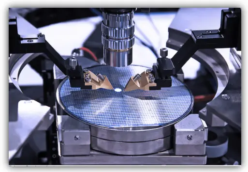
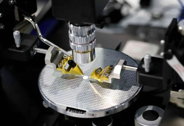
Materials used in semiconductor CNC machining
In semiconductor CNC (Computer Numerical Control) machining, precise and controlled cuts are made using specialized machinery and materials. Some common materials used in this process include silicon, gallium arsenide, germanium, sapphire, and ceramics. Each of these materials has unique properties and is used for specific applications in the semiconductor industry.
Silicon: Silicon is the most commonly used material in the semiconductor industry due to its abundance, low cost, and excellent electrical properties. It is often used to create microelectronic devices such as computer chips and solar cells.
Gallium Arsenide: Gallium arsenide is a semiconductor material that has higher electron mobility than silicon, making it ideal for high-speed devices such as lasers and radar systems.
Germanium: Germanium is a semiconductor material that has higher electron mobility than silicon and is often used in optoelectronic devices such as lasers and infrared detectors.
Sapphire: Sapphire is a hard, transparent material that is often used in the semiconductor industry due to its high strength and resistance to wear and corrosion. It is often used to create windows and protective coatings for electronic devices.
Ceramics: Ceramic materials are often used in the semiconductor industry due to their excellent mechanical and electrical properties. They are often used to create components such as substrates and packaging materials.
Types of semiconductor machining
There are several different types of semiconductor machining processes that are used to create and modify microscale components for the semiconductor industry. These processes include wafer sawing, photolithography, wet etching, dry etching, ion implantation, and deposition. Each of these processes has specific applications and is used to achieve specific results in the manufacturing of semiconductor components.
Wafer sawing: This process involves using a diamond blade to cut thin wafers into smaller pieces or to create specific shapes.
Photolithography: This process involves using light to transfer a pattern onto a photosensitive material, which is then used as a mask to etch or deposit material onto a substrate.
Wet etching: This process involves using chemicals to etch away material from the surface of a component. This is often done using a liquid solution and can be used to create specific shapes or patterns.
Dry etching: This process involves using physical or chemical means to remove material from the surface of a component without the use of a liquid solution. This can be done using processes such as plasma etching or reactive ion etching.
Ion implantation: This process involves using a high-energy beam of ions to implant them into the surface of a component. This is often done to alter the electrical properties of the material.
Deposition: This process involves adding material to the surface of a component, either through physical vapor deposition (PVD) or chemical vapor deposition (CVD). This can be used to add protective coatings or to create specific patterns or structures.
Challenges and considerations in semiconductor CNC machining
Semiconducting CNC machining involves working with extremely small and precise components, which presents a number of challenges and considerations. These include the need to work with micro scale sizes and tolerances, the complexity of shaping and designing complex components, and the difficulties of working with brittle and hard materials. In addition, ensuring the quality and accuracy of the finished product is of utmost importance, and strict measures must be taken to prevent contamination and maintain efficiency. There are also environmental considerations, such as the impact of machining processes on air and water quality.
Microscale size and tolerances: Semiconductor components are extremely small, often on the order of micrometers or even nanometers. Working with such small scales requires extremely precise machinery and techniques, as even small deviations can have a significant impact on the performance of the finished product.
Complex shapes and designs: Semiconductor components often have complex shapes and designs, which can be challenging to create and modify using CNC machining. This requires precise control and the use of specialized machinery and techniques.
Working with brittle and hard materials: Many of the materials used in semiconductor CNC machinings, such as silicon and sapphire, are brittle and hard, which can make them difficult to work with. This requires the use of specialized cutting tools and techniques to prevent damage to the material.
Quality control measures: Ensuring the quality and accuracy of the finished product is critical in the semiconductor industry. Strict quality control measures must be in place to ensure that components meet the required specifications and performance standards.
Precision and accuracy: Semiconductor CNC machining requires extreme precision and accuracy to create components that meet the required specifications. This requires the use of specialized machinery and techniques to achieve the necessary tolerances.
Contamination control: Contamination is a major concern in the semiconductor industry, as even small amounts of foreign materials can significantly impact the performance of the finished product. Strict measures must be taken to prevent contamination during the machining process.
Cost and efficiency: The cost and efficiency of the machining process are important considerations, as the semiconductor industry is highly competitive. It is important to find ways to reduce costs and improve efficiency while maintaining the necessary quality and precision.
Environmental impact: The semiconductor industry has a significant environmental impact, including air and water pollution from machining processes. It is important to consider the environmental impact of these processes and find ways to minimize their negative effects.
Common CNC machined Semiconductor Parts
Semiconductor CNC machining is used to create a wide range of microscale components for use in the semiconductor industry. These components are used in a variety of applications, including microelectromechanical systems (MEMS), microfluidic devices, optoelectronic devices, and integrated circuits (ICs).
Microelectromechanical systems (MEMS): These are small mechanical devices that are created using semiconductor materials and are used in a wide range of applications, including sensors, actuators, and microelectronic components.
Microfluidic devices: These are small devices that are used to manipulate and analyze fluids at the microscale. They are often used in the medical and biotech industries for applications such as drug delivery and tissue engineering.
Optoelectronic devices: These are devices that are used to convert electrical and optical signals. They are often used in applications such as lasers and infrared detectors.
Integrated circuits (ICs): These are microelectronic devices that are created using semiconductor materials and are used to process and store information. They are the building blocks of electronic devices such as computers and smartphones.
Applications of semiconductor machining
Semiconductor machining is used to create a wide range of microscale components that are used in a variety of applications. These components are used in electronic devices such as computers and smartphones, solar cells, medical equipment, and aerospace and defense systems. Semiconductor machining plays a vital role in the creation of these components, as it allows for the precise and controlled creation of microscale components to precise specifications. These components are the building blocks of modern technology and are essential for the development and advancement of a wide range of technologies.
Computer chips: Semiconductor CNC machined components are used to create computer chips that power laptops, desktops, and other electronic devices.
Smartphones and other electronic devices: These components are used in the creation of a wide range of electronic devices, including smartphones, tablets, and other consumer electronics.
Solar cells: Semiconductor CNC machined components are used to create the photovoltaic cells that make up solar panels, which are used to generate clean energy.
Medical equipment: These components are used in the creation of medical devices such as pacemakers, insulin pumps, and imaging equipment.
Aerospace and defense systems: Semiconductor CNC machined components are used in a variety of aerospace and defense applications, including radar systems, satellite communication systems, and missile guidance systems.
Conclusion
Looking to the future, it is likely that advancements and innovations in semiconductor machining will continue to drive the development of new technologies and improve our quality of life. As the demand for electronic devices and systems continues to grow, the semiconductor industry will play an increasingly important role in driving innovation and enabling the development of new technologies.
If you are in need of high-quality semiconductor CNC machining services, look no further! Our team of experienced professionals is dedicated to providing the best possible results for your specific needs. We use state-of-the-art machinery and techniques to ensure that your components meet the highest standards of quality and precision. Contact us today to learn more about how we can help you with your semiconductor machining needs!